Reveal for Lattice FPGA Debugging Tutorial [Guide]
You’re wrestling with a complex Lattice FPGA design, and suddenly, your project grinds to a halt. A bug’s lurking somewhere in your code, but where?
Enter Reveal, Lattice’s integrated logic analyser – your handy tool for FPGA debugging.
Here we provide some top tips on how to get the most out of Reveal for Lattice FPGA Debugging.
TL; DR
- Reveal is Lattice’s integrated logic analyser that gives you “X-ray vision” into your running FPGA design
- Engineers spend ~44% of development time debugging – mastering Reveal can significantly reduce this
- Capture and analyse real-time signals without the need for external test equipment
- Set complex trigger conditions to catch elusive bugs that traditional methods might miss
- Debug across multiple clock domains with precise timing analysis
- Identify performance bottlenecks and optimisation opportunities within your design
- Particularly valuable for debugging high-speed interfaces like MIPI CSI-2
- Requires proper setup including JTAG configuration (we’ll show you exactly how)
- Our real-world case study demonstrates decoding MIPI video formats that would be nearly impossible without Reveal
Contents
Let’s face it: debugging FPGAs can be a right pain. You’re dealing with intricate designs, multiple clock domains, and high-speed interfaces. It’s like trying to find a needle in a haystack, except the needle keeps moving.
That’s where Reveal comes in handy.
Reveal isn’t just another debugging tool; it’s a game-changer for Lattice FPGA development. It lets you peek inside your design while it’s running, giving you real-time insights without the need for external equipment. Imagine having X-ray vision for your FPGA.
According to a survey by Wilson Research Group, verification engineers spend about 44% of their time debugging. That’s a massive chunk of your development cycle. By mastering Reveal, you’re not only solving problems faster; you’re potentially shaving weeks off your project timeline.
What is Reveal? Understanding Lattice's Integrated Logic Analyser
So, what exactly is Reveal?
Simply put, it’s a built-in logic analyser that comes with Lattice’s design tools.
But don’t let its integration fool you – Reveal packs a punch.
Reveal allows you to insert debug cores into your design, capture real-time data, and analyse it without disrupting your FPGA’s normal operation. It’s like having a microscope that doesn’t interfere with the specimen you’re studying.
Key features – Reveal offers:
- Real-time signal capture
- Complex trigger conditions
- Multi-clock domain support
- Integration with Lattice Diamond and Radiant software
Reveal offers seamless integration with Lattice’s ecosystem. This avoids juggling multiple software packages or dealing with compatibility issues.
A study by Mentor Graphics (now part of Siemens) found that integrated debugging tools can reduce debug time by up to 50%. A potential project-saver when you’re up against tight deadlines. But Reveal is a powerful tool for optimising your design. By analysing signal behaviour in real-time, you can spot performance bottlenecks and inefficiencies that might otherwise go unnoticed.
Of course, effective debugging isn’t just about fixing what’s broken. It’s about understanding your design inside and out.
And that’s exactly what Reveal helps you achieve.
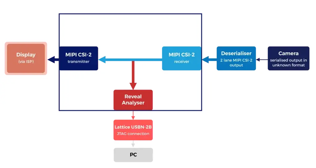
Real-world Crosslink Plus case study: MIPI packet debugging
A recent project required the reception of a video stream from a camera, so that it could be converted to YUV422 for external use. The incoming video stream was in an unknown format and needed investigation before the conversion stage of the project could begin.
Lattice’s Reveal tool made it possible to decode the video format (Data Identifier) from the MIPI stream. This would otherwise have been a difficult task without specialist decoding equipment.
Setting Up Reveal for Your Lattice FPGA Project
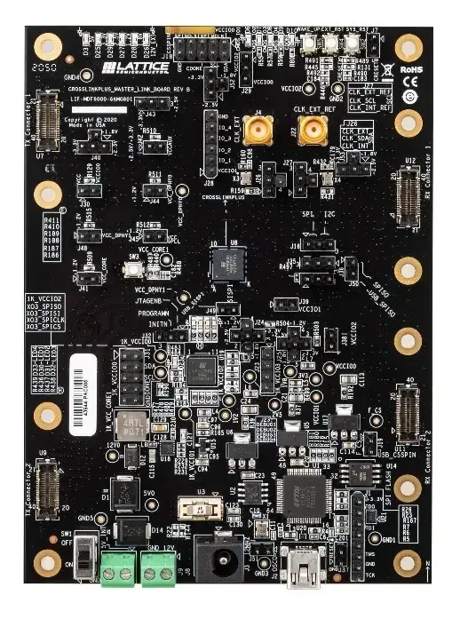
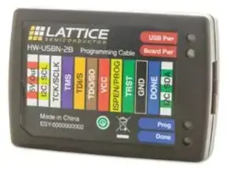
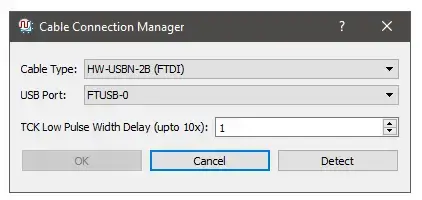
The Lattice HW-USBN-2B programmer was used to load the configuration data into the CrosslinkPlus. The JTAG pins were also connected to GPIO on the Crosslink for Reveal Analyser use.
Originally this design only included an I2C connection to the FPGA for programming. We realised that, although the CrosslinkPlus plus doesn’t have dedicated JTAG pins, we still needed a JTAG port to use reveal. This was achieved with a soft-JTAG port using spare IO pins that weren’t otherwise used in the design. Until you insert the Reveal Analyser into your design, it isn’t immediately obvious how to assign soft JTAG pins.
It was found that the camera was sending Embedded 8-bit non-Image Data, at the beginning of each frame, which was triggering the Analyser. Initially there was some concern that the entire frame was being sent in this format, making any kind of format conversion very difficult. Using Trigger Expression logic, it was possible to filter out the non-image data.
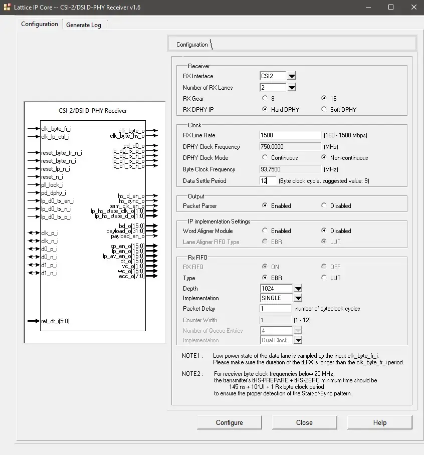
To access the MIPI video format and data payload, the Packet Parser is enabled when setting up the IP core in Clarity:
The DPHY core requires a 100MHz input clock, so it should be ensured that an appropriate source is provided. This system example used a 25MHz input clock that fed a PLL.
The Reveal inserter can only be used with a JTAG interface, but as the CrosslinkPlus (LIFMD) has no dedicated JTAG port, it is necessary to define GPIO to perform this function.
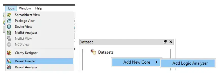
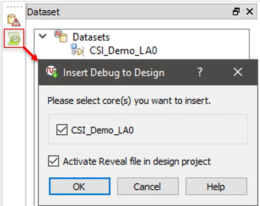
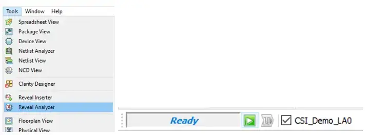
The JTAG port pins must be manually assigned, but the logic will be automatically added when Reveal is inserted into the design. Open the reveal inserter from the tools menu and add a new Logic Analyser by right clocking in the Datasets box.
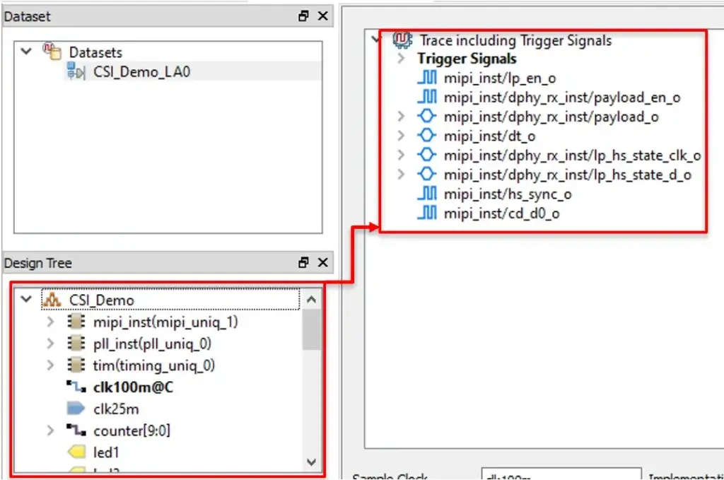
The signals to be monitored are added from the Design Tree and dragged into the Trace window. These signals are defined in the Lattice IP Core csi2/dsi d-phy receiver v1.6, which is installed through the Clarity tool:
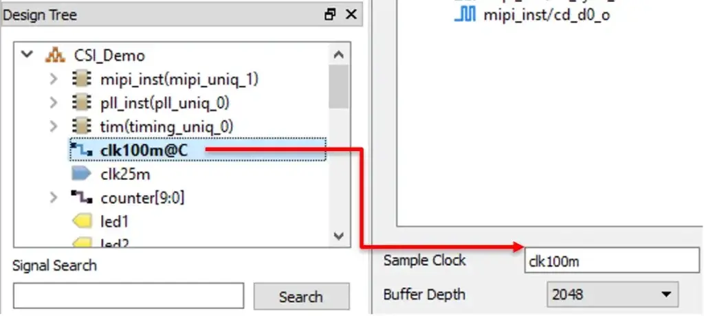
Add the sample clock for the analyser; in this case, a 100 MHz PLL output was used:
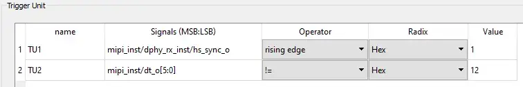
Next pick the signals to be used for triggering, in this case “hs_sync_o” worked best. This is done by adding a Trigger Unit in the Trigger Signal Setup tab of the inserter:
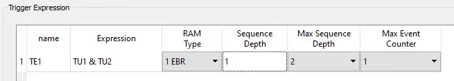
In some cases, camera MIPI data may contain different data format types and so it is useful to add an expression to remove any data that is not of interest.
A Trigger Expression is added in a similar way and can be used to combine Trigger units. In this case we are only triggering on the rising edge of hs_sync_o, when the video data indentifier is not 0x12:
Once all the required triggers and signals have been added, inset the debugger into the design:
In Spreadsheet View the JTAG port should have been added, it just needs pins assigning.
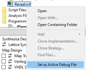
Make sure the Reveal Inserter is set as active (shown in bold):
Ensure the programmer has been detected by Lattice Diamond, then program the device over I2C.

Once programmed successfully, open the Reveal Analyser and run the debugger:
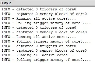
If running successfully (with no trigger stimulus) you will see receive polling messages in the output
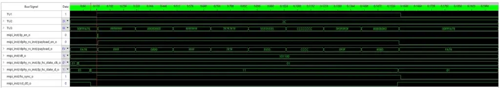
Enabling the camera video stream should trigger the analyser, and a line of data should be captured:
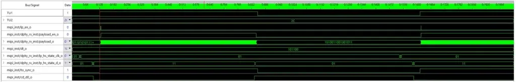
A payload should then be visible with the data type shown in both the TU2 and dt_o rows. The red cursor shows the trigger point on the rising edge of hs_sync_o.
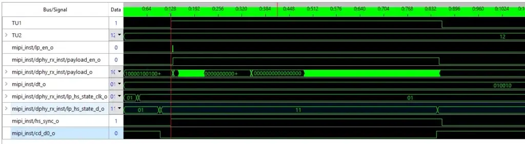
Further tests were done with the camera generating a test pattern:
The Embedded 8-bit non-Image Data that was initially triggering the analyser is shown below:
The design initially used a soft DPHY on GPIOs, but RX Line rate limitations meant that the RAW12 video data was not captured.
After a hardware modification, the dedicated Hard DPHY pins were used enabling a line rate of 1500Mbps using.
The limitations of the Crosslink soft DPHYs should be considered when designing a system that uses them.
Optimising FPGA Performance with Reveal Insights
Now that you’ve mastered the art of debugging with Reveal, let’s use these insights to squeeze every last drop of performance from your Lattice FPGA.
By analysing the data you capture, you can spot bottlenecks and inefficiencies that might otherwise go unnoticed.
Here’s how to make the most of your Reveal insights:
- Identify critical paths: Use Reveal to monitor your design’s critical paths in real-time. This can help you spot timing issues before they become problems.
- Optimise resource utilisation: By examining signal activity, you can identify unused or underused resources. This can free up valuable FPGA real estate for other functions.
- Fine-tune clock domains: Reveal’s multi-clock domain support is brilliant for optimising clock relationships and minimising skew.
- Optimisation is a balancing act. You’re juggling performance, resource utilisation, and power consumption. It’s like trying to solve a Rubik’s cube blindfolded – tricky, but not impossible with the right tools.
Caution: don’t get caught up in premature optimisation. As the old engineering adage goes, “Make it work, make it right, make it fast – in that order.”
Conclusion: Mastering FPGA Debugging with Reveal
Key takeaways:
- Start small and scale up your debug setup as needed.
- Use complex triggers to catch elusive bugs.
- Leverage Reveal’s multi-clock domain support for comprehensive debugging.
- Integrate Reveal with other tools for a holistic debugging approach.
- Use Reveal insights to optimise your FPGA design’s performance.
By incorporating Reveal into your regular development practices, you’re not only fixing bugs – you’re elevating your entire FPGA design process. You’re transforming from a code wrangler into a silicon whisperer.
The ability to quickly identify and resolve issues can make or break a project. With Reveal in your toolkit, you’re well-equipped to tackle whatever challenges come your way.
Ready to Supercharge Your FPGA Debugging?
Whether you're wrestling with complex timing issues or hunting down elusive glitches,
we've got the expertise to help you conquer any FPGA challenge.
Get in touch today to discover how ByteSnap can turbocharge your FPGA development process.
Let's work together to bring your innovative designs to life, faster and more efficiently than ever before.
Founded in 2008, ByteSnap Design is an award-winning embedded systems design consultancy, offering a comprehensive range of services across the electronic product development lifecycle.
A highly skilled team of over 40 hardware and software engineers, our expertise spans several sectors, including IoT, automotive, industrial, medical, and consumer electronics.
The engineering consultants on the ByteSnap Editorial Team share their knowledge and practical tips to help you streamline your product development and accelerate designs to market successfully.
With their deep technical expertise and practical experience, they aim to provide valuable insights and actionable tips to guide you through the complex world of electronic product design and development, to help you bring innovative, reliable, and secure electronic products to market quickly and cost-effectively.